
Dicing Services for Hybrids and Semiconductors
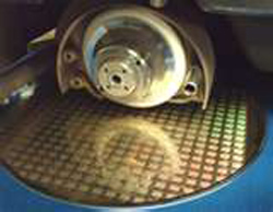
Precision custom dicing, backgrinding and slicing services are provided by for both dicing process development as well as high volume contract dicing requirements. Dicing saws are fully programmable and equipped with high power microscopes for precision alignment.
Accurate dicing services for customer materials up to 6" in diameter or square and rectangles as large as 6"x14". Materials processed are as diverse as Fused Silica, Silicon wafers, Glass, Sapphire and Quartz disks, Silicon Carbide, Ferrites, Ceramics, MEMS and hybrid circuits as well as delicate compound semiconductors like GaN and InP. Many of these wafers and materials are in stock.
Custom dicing capabilities can also extend the services of your wafer fab enabling you to handle production pressures as we meet your requirements for kerf, chip specifications, and delivery. Depending upon the material, the dicing kerf may be as small as .001" and die size as small as .005" square.
Additional cutting-dicing services include slotting, singulating, angling and cutting through layered assemblies like Silicon-on-Glass, machining grooves, Sapphire, glass and metal rod cutting and rough cutting of plates as large as 18" x 18". Valley also provides backlapping and thinning services for wafers up to 12" diameter, along with lapping and commercial or optical polishing of most materials, edge polishing , and polishing of semiconductor wafers up to 300mm in diameter.
For a complete summary of dicing capabilities click here.
Please click here for a dicing quotation per your specifications.
Informative related Web sites:
- www.semi.org Semiconductor Equipment and Materials
- www.edgepolishing.com Polishing edges and edge angles
- www.aluminumnitride.com Aluminum Nitride Ceramic substrates
- www.valleydesign.com Electro-Optical materials processing for microelectronics, Fiber Optics, optics and semiconductor industries
- www.imaps.org IMAPS International Microelectronics and Packaging Association for advancement of microelectronics and electronic packaging
- www.ultra-thin.com Thinning of all hard materials to micron thickness
- www.laserslag.com Laser slag removal from lasered Aluminum Nitride and Aluminum Oxide Ceramic Substrates
- www.quartz-silica.net Fused Silica and Fused Quartz wafers custom made and also from extensive finished stock
- www.siliconwafers.net Specializing in ultra-tight tolerance wafers and float zone optical grade Silicon materials
- www.sapphirewafers.com Sapphire wafers and substrates
- www.germaniumcrystals.com Germanium Ge infrared optical components and windows
- www.customdicing.com/wafer-dicing Wafer dicing, sawing, singulating and backgrinding
|
Go to valleydesign.com |
|